|
Understanding the Functionality of Your Motherboard Chipset
The chipset consists of two main components, the North- and South- Bridge chips,
which are connected over the PCI bus. The CPU, Memory and AGP talk to the Northbridge and the
Southbridge handles all the I/O, including the ISA bus.
The link between the CPU and
Northbridge is called Front-side bus, which is (usually) the same speed as the Memory Bus, and can
be varied, as when overclocking. The Back-side bus connects the CPU with L2 cache.
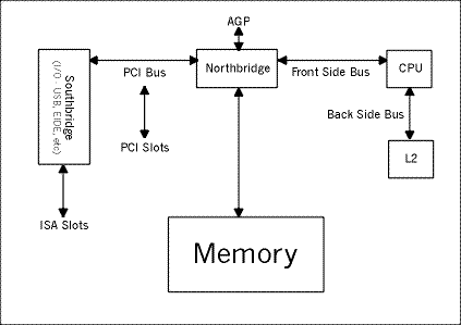
Simplified picture of a
PC-compatible motherboard.
But even this is changing, because the essential problems that plagued the original
PC still haven't gone away, in that some parts of the machine simply run too slowly, notably the
PCI bus, which, at 33 MHz, is 10 times slower than even a 333 MHz CPU. If that weren't bad enough,
all the I/O, including USB and Firewire, go through the Southbridge and hence the PCI bus, losing
all that speed advantage.
Intel's intention (starting with 800 series chipsets) is to have
three major components, namely a memory controller hub, an I/O controller hub and a firmware hub,
all tied together with a 266 Mbps interface. The CPU and AGP would talk directly to the memory
controller, and any ISA slots would run through the firmware hub.
This is an article from
Phil Croucher, author of
"The BIOS Companion" Phil has a way
of explaining in "plain" English. The information is well presented and is well above A+
standard.

|